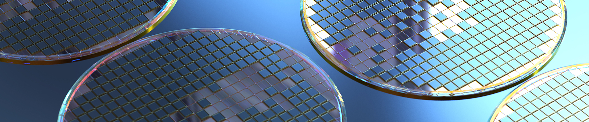
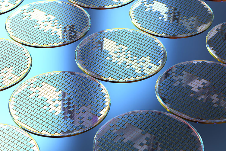
Semiconductors Front-end
manufacturing process
Semiconductors Front-end manufacturing process
-
 AnnealingClick here!
-
 CVD DepositionClick here!
-
 PhotolithographyClick here!
-
 EtchingClick here!
-
 Ion ImplantationClick here!
-
 PVD CoatingClick here!
-
 CMP PolishingClick here!
-
 CleaningClick here!
 -

Semiconductors Facilities systems
-
 AnnealingClick here!
-
 CVD DepositionClick here!
-
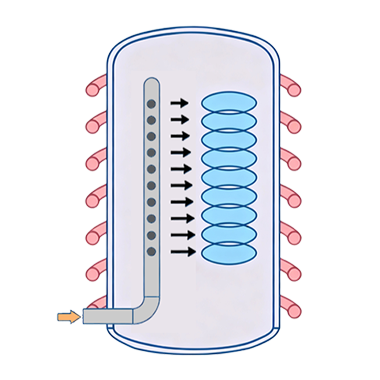
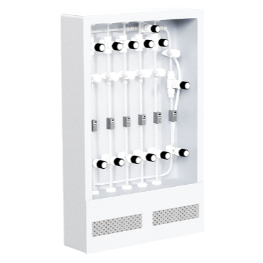 CDS liquid supply systemClick here!
-
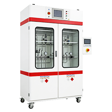
AnnealingThe oxidation process generates a silicon dioxide (SiO ₂) layer by reacting silicon with oxygen (O ₂) or water vapor (H ₂ O) at high temperatures, which is used as a gate dielectric or isolation layer; The annealing process repairs lattice damage, activates doped atoms, or optimizes film properties by heating (such as rapid thermal annealing RTA).
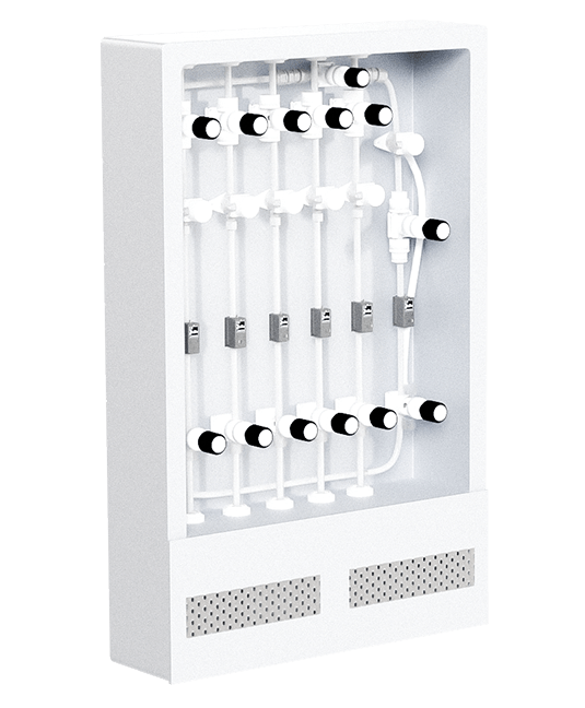
The key equipment for oxidation annealing process is vertical furnace and rapid heat treatment equipment (RTP), each equipped with 4-6 working units (PM), each PM including 1 cooler, 1 pump, and 1 gas box. Nitrogen (N ₂), hydrogen (H ₂), or inert gas (Ar) are commonly used to control the reaction environment during the processing.
-
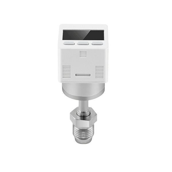
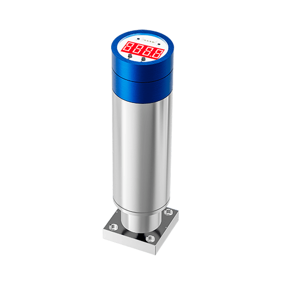
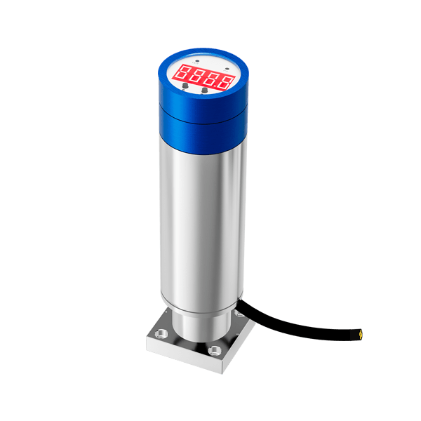
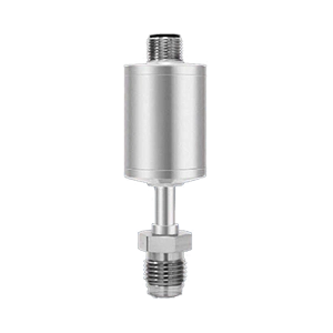
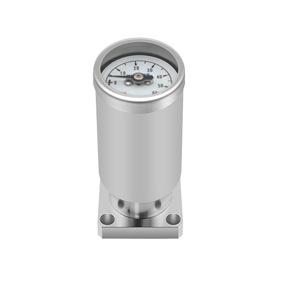
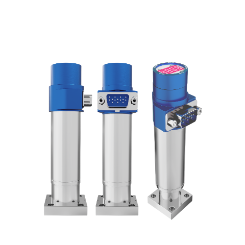
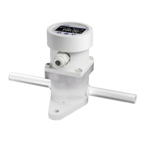
Recommended Products
-
-
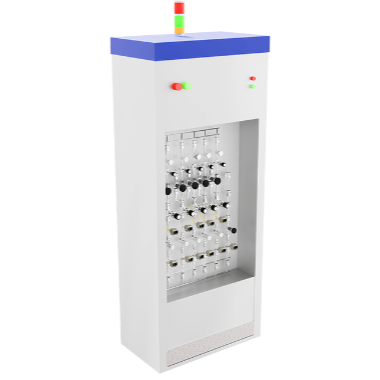
CVD DepositionChemical Vapor Deposition (CVD) is a key semiconductor process that deposits thin films (e.g., SiO₂, Si₃N₄, polysilicon) on wafer surfaces through gas-phase chemical reactions. Reactive gases such as SiH₄ and NH₃ are introduced into the chamber and decomposed under high temperature or plasma to form dense, uniform films. It is used for gate dielectrics, interconnects, and passivation layers.
CVD includes LPCVD (Low-Pressure), PECVD (Plasma-Enhanced), and ALD (Atomic Layer Deposition). Each tool has 4–6 process modules (PM), and each PM uses 4–15 types of gases and sensors.
-
Recommended Products
-
-
PhotolithographyPhotolithography precisely transfers circuit patterns from a reticle onto the photoresist on the wafer surface, achieving nanometer-level accuracy. It is the most precise process in semiconductor manufacturing.
Key equipment includes DUV lithography systems, EUV lithography systems, and coat-develop tracks.The process flow consists of substrate preparation, coating, soft bake, exposure, development, hard bake, and inspection/metrology, during which gas and liquid pressure and flow are continuously monitored to ensure process stability.
-
Recommended Products
-
-
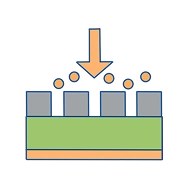
EtchingEtching selectively removes materials not protected by photoresist through physical or chemical methods, accurately transferring patterns from the photoresist to the substrate to form circuit structures.
Dry etching systems use various gases (such as HBr, Cl₂, and SF₆) to etch wafers. Each etching tool is equipped with 3–6 plasma-enhanced etching modules (PM), and each PM includes about 18 gas lines and pressure sensors.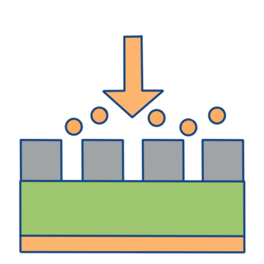
-
Recommended Products
-
-
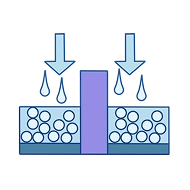
Ion ImplantationIon implantation bombards the wafer surface with a high-energy ion beam to implant dopant atoms (such as B, P, or As) into the silicon lattice, forming PN junctions or adjusting threshold voltages to modify device electrical characteristics.
The ion source generates the ion beam using gases such as B₂H₆, BCl₃, BBr₃, PCl₃, and AsCl₃.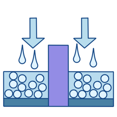
-
Recommended Products
-
-
PVD CoatingPhysical Vapor Deposition (PVD) uses physical methods such as sputtering or evaporation to convert solid target materials into vapor and deposit them onto the wafer surface, forming metallic or dielectric films (e.g., Al, Cu, TiN) for interconnects, electrodes, or diffusion barrier layers. It is a key metallization process in semiconductor manufacturing.
Different processes use different gases, but PVD typically requires fewer gases and sensors.
-
Recommended Products
-
-
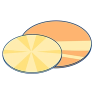
CMP PolishingCMP achieves global planarization of the wafer surface through the combined action of chemical etching and mechanical polishing. The downforce of the polishing head is controlled by CDA pressure, and HF, N₂, and deionized water are used for wafer cleaning and drying. Post-CMP cleaning uses different solutions and methods as required, while gas and liquid pressure and flow are monitored throughout the process.
-
Recommended Products
-
-
CleaningCleaning removes particles, organic residues, metal contaminants, and oxide layers from the wafer surface to ensure interface quality for subsequent processes. It is a key step in contamination control. Cleaning tools use chemicals such as ultrapure water, acids, and gases to clean wafers, while the chemical modules monitor and control the flow and pressure of chemicals, water, and gases.

-
Recommended Products
-
-
AnnealingThe oxidation process generates a silicon dioxide (SiO ₂) layer by reacting silicon with oxygen (O ₂) or water vapor (H ₂ O) at high temperatures, which is used as a gate dielectric or isolation layer; The annealing process repairs lattice damage, activates doped atoms, or optimizes film properties by heating (such as rapid thermal annealing RTA).
The key equipment for oxidation annealing process is vertical furnace and rapid heat treatment equipment (RTP), each equipped with 4-6 working units (PM), each PM including 1 cooler, 1 pump, and 1 gas box. Nitrogen (N ₂), hydrogen (H ₂), or inert gas (Ar) are commonly used to control the reaction environment during the processing.
-
CVD DepositionThe oxidation process generates a silicon dioxide (SiO ₂) layer by reacting silicon with oxygen (O ₂) or water vapor (H ₂ O) at high temperatures, which is used as a gate dielectric or isolation layer; The annealing process repairs lattice damage, activates doped atoms, or optimizes film properties by heating (such as rapid thermal annealing RTA).
The key equipment for oxidation annealing process is vertical furnace and rapid heat treatment equipment (RTP), each equipped with 4-6 working units (PM), each PM including 1 cooler, 1 pump, and 1 gas box. Nitrogen (N ₂), hydrogen (H ₂), or inert gas (Ar) are commonly used to control the reaction environment during the processing.
-
CDS liquid supply systemThe oxidation process generates a silicon dioxide (SiO ₂) layer by reacting silicon with oxygen (O ₂) or water vapor (H ₂ O) at high temperatures, which is used as a gate dielectric or isolation layer; The annealing process repairs lattice damage, activates doped atoms, or optimizes film properties by heating (such as rapid thermal annealing RTA).
The key equipment for oxidation annealing process is vertical furnace and rapid heat treatment equipment (RTP), each equipped with 4-6 working units (PM), each PM including 1 cooler, 1 pump, and 1 gas box. Nitrogen (N ₂), hydrogen (H ₂), or inert gas (Ar) are commonly used to control the reaction environment during the processing.